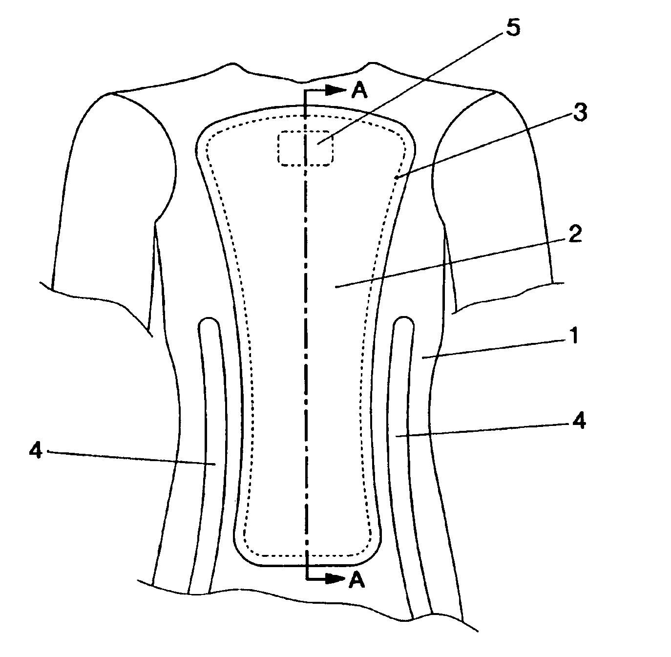
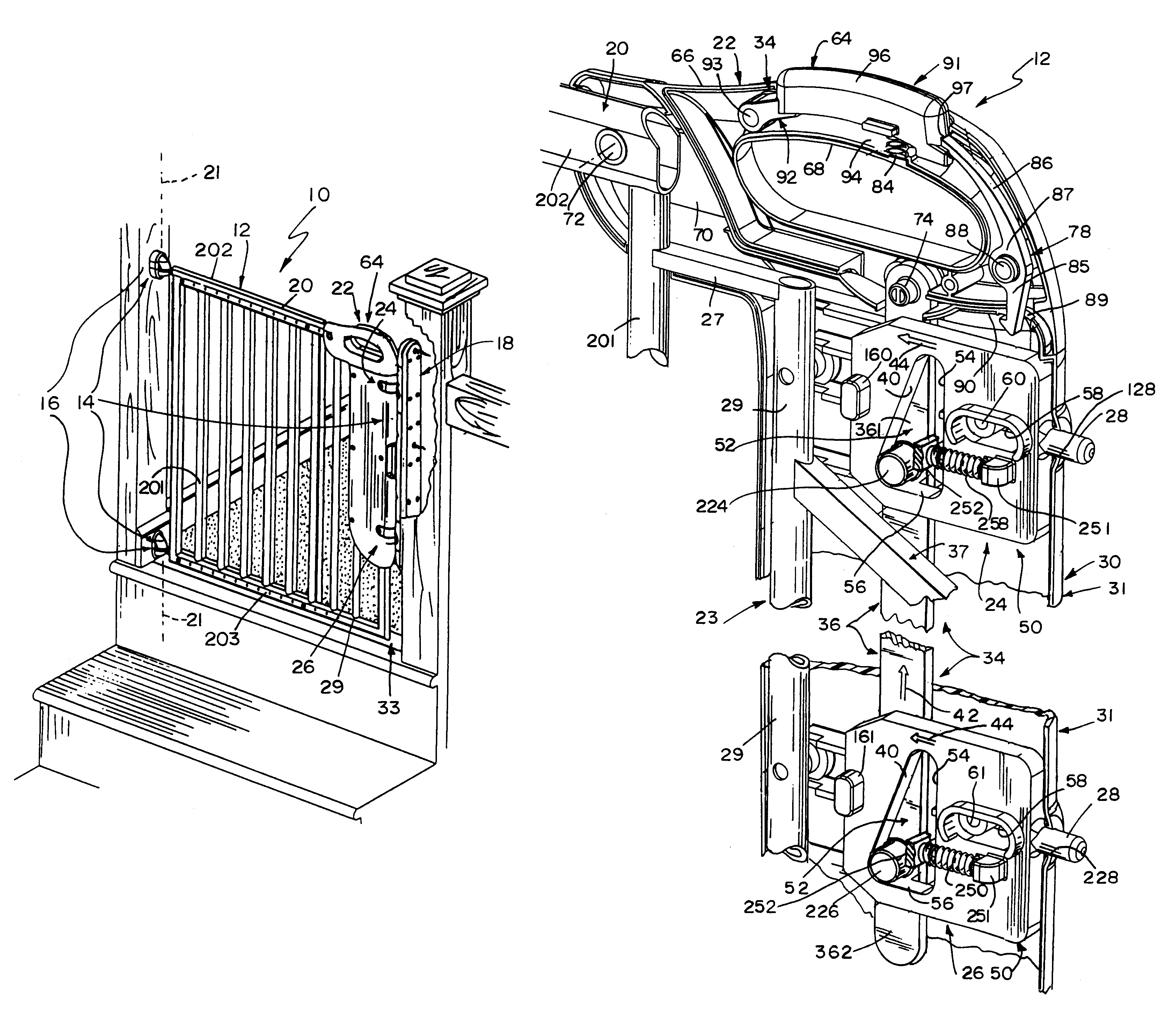
Today’s Patent – Semiconductor device having a superlattice and punch through stop (PTS) layers at different depths and related methods
The said invention (CN107771355B) was invented by R.J. Myers, Hideki Takeuchi patented by
CNIPA on 14-01-2022. Currently, it stands assigned to Atomera Inc.
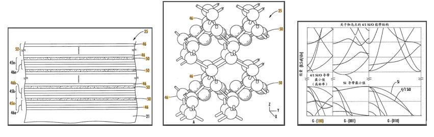
This invention enhances transistor performance by optimizing charge control and leakage
prevention. Traditional semiconductor designs faced challenges like excessive leakage currents and
reduced efficiency due to poor electron confinement. This innovation strategically places
superlattice and PTS layers at different depths, improving charge carrier mobility, reducing
leakage, and enhancing device reliability. Compared to earlier technologies, it enables higher-speed
operation, lower power consumption, and improved thermal stability, making it ideal for
advanced processors and memory chips. This breakthrough significantly advances semiconductor
efficiency, boosting performance in modern electronics.


 +1 888 890 6411