Today’s Patent – Semiconductor Device and Manufacturing Method Thereof
The said invention (US12191148B2) was invented by Yasunori Agata, Takashi Yoshimura, Hiroshi TAKISHITA, Misaki MEGURO, Naoko Kodama, Yoshihiro Ikura, Seiji Noguchi, Yuichi Harada, Yosuke Sakurai, and patented by USPTO on July 20th, 2024. Currently, it stands assigned to the Fuji Electric Co Ltd.
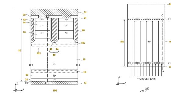
This invention relates to a semiconductor device featuring a carefully engineered donor concentration profile across the depth of a semiconductor substrate.
The device includes a first donor concentration peak near the lower surface, a second, lower peak closer to the upper surface, and a flat region of substantially uniform donor concentration between them, comprising at least 10% of the substrate’s thickness. Additional donor peaks may be distributed below the first peak. This structure enhances device performance by enabling controlled carrier distribution and improving breakdown voltage and switching characteristics.
The donor concentration profile may be coordinated with hydrogen implantation, creating overlapping donor and hydrogen peaks at specific depths, with tailored slopes and concentration gradients. The device may incorporate active regions such as transistors, diodes, or gate trenches, where donor profiles are strategically located. Methods of fabrication include sequential hydrogen implantation and thermal diffusion to form the desired concentration regions, enabling high-performance devices such as IGBTs or MOSFETs with precise electrical characteristics.


 +1 888 890 6411